Down to Atoms

Scanning electron, atomic force & scanning tunneling microscopy · 2018–2019

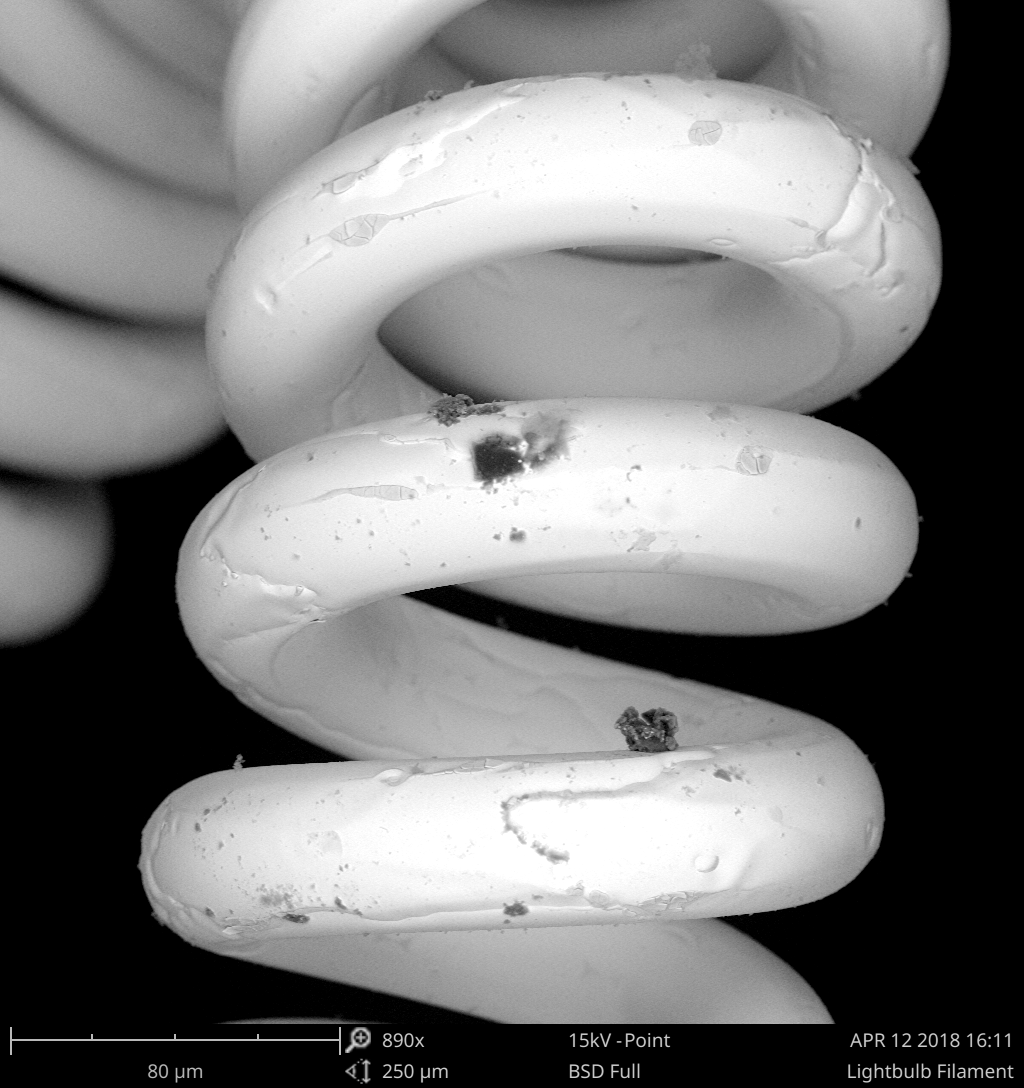
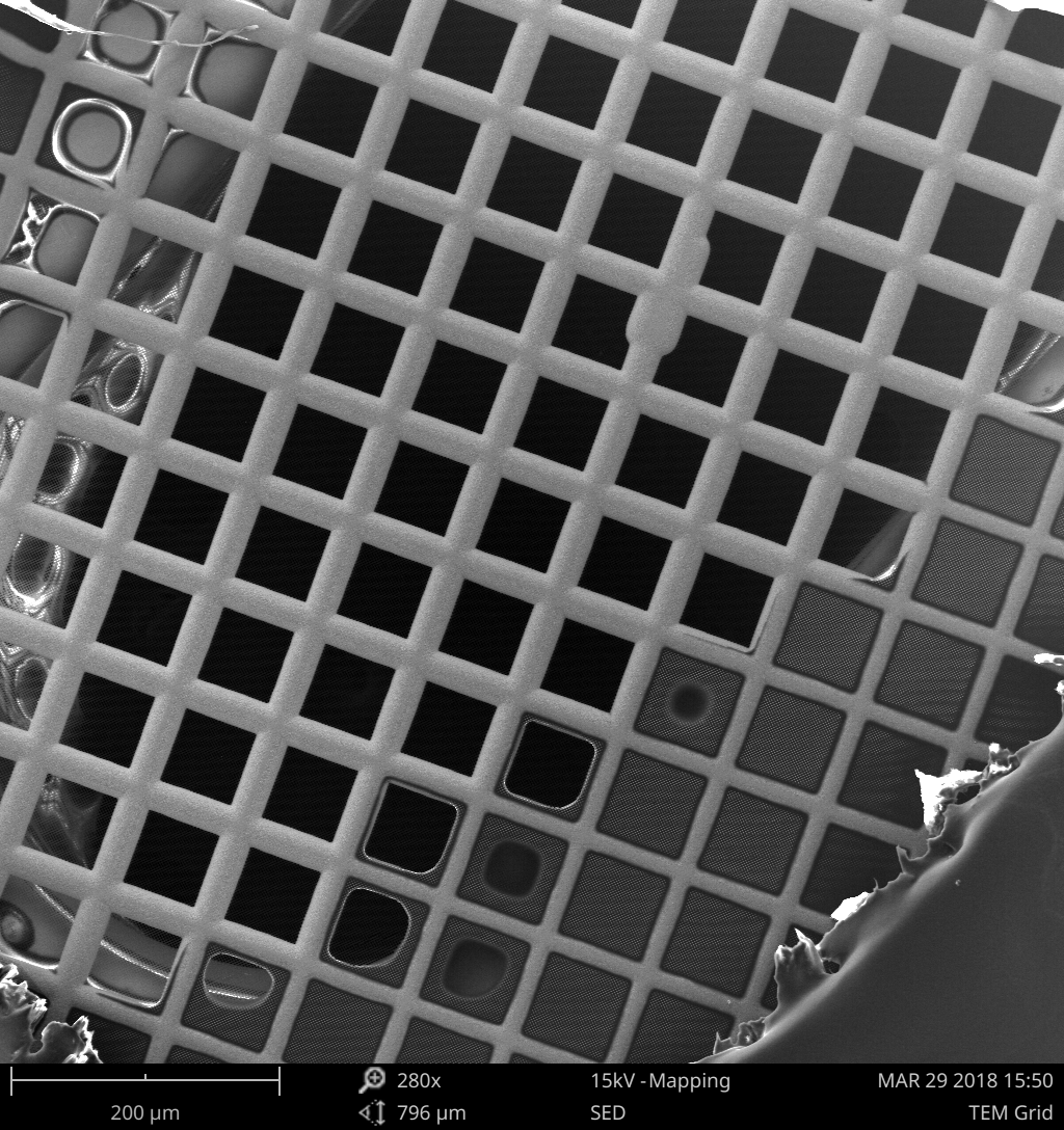
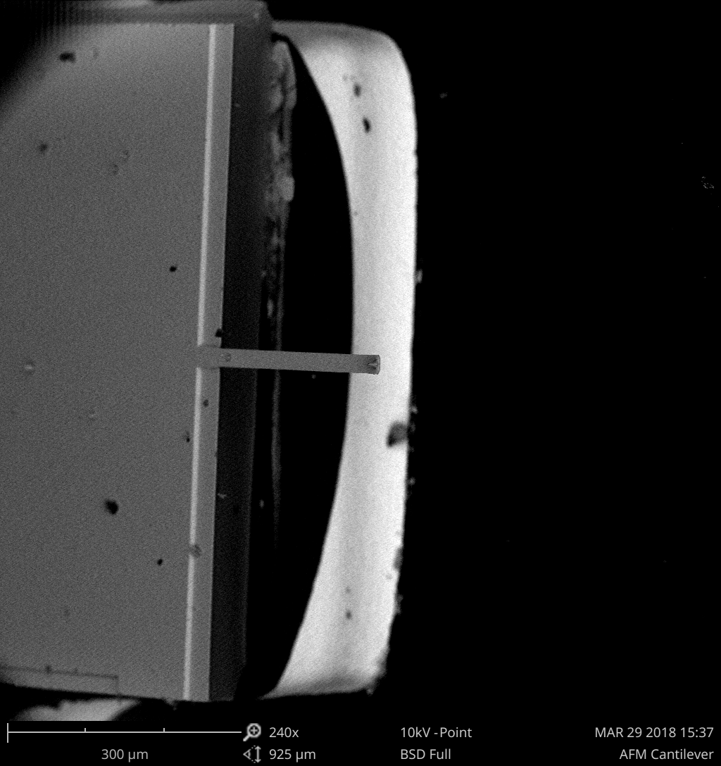
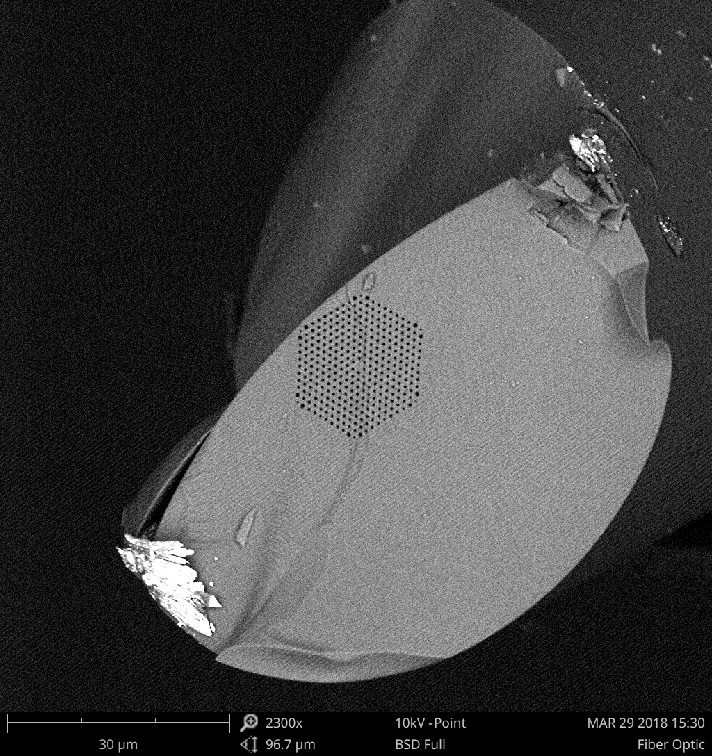
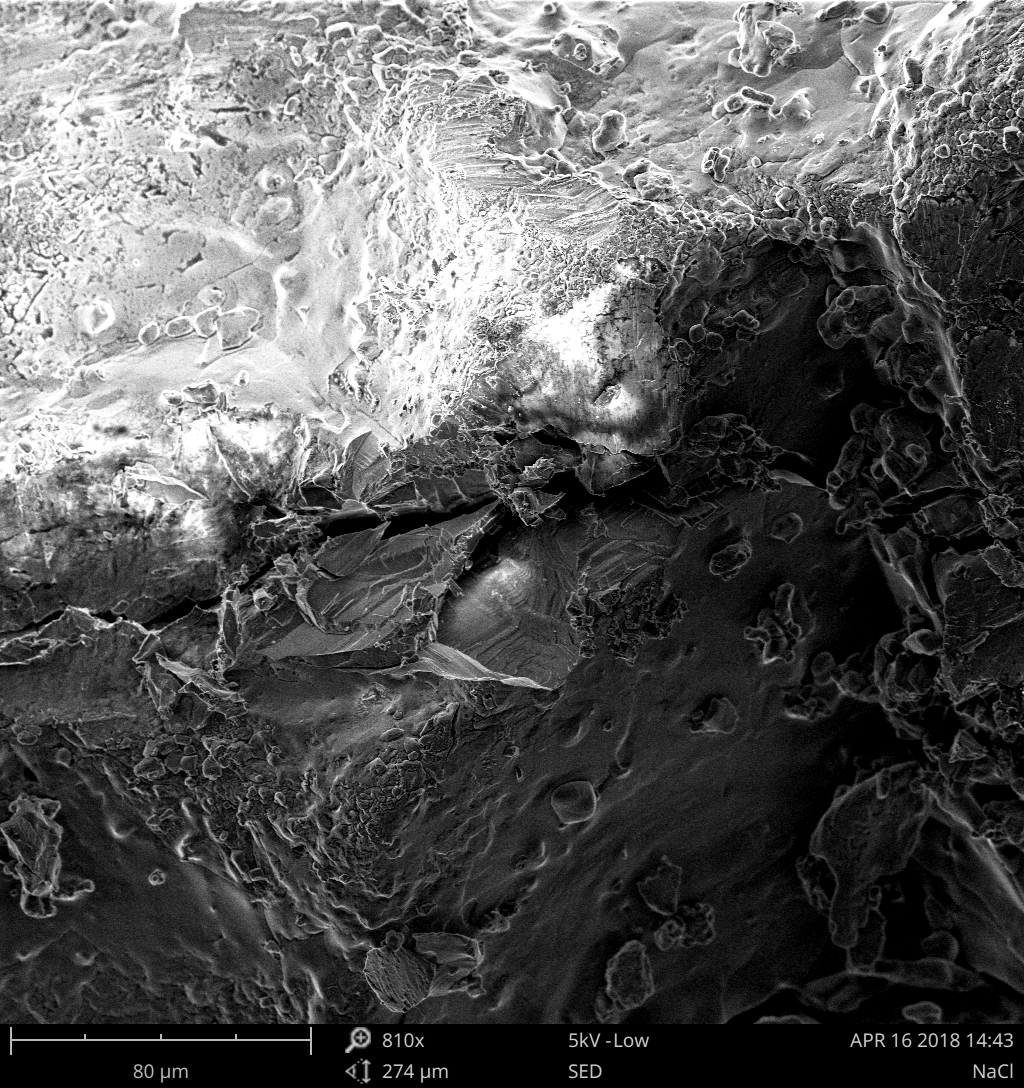
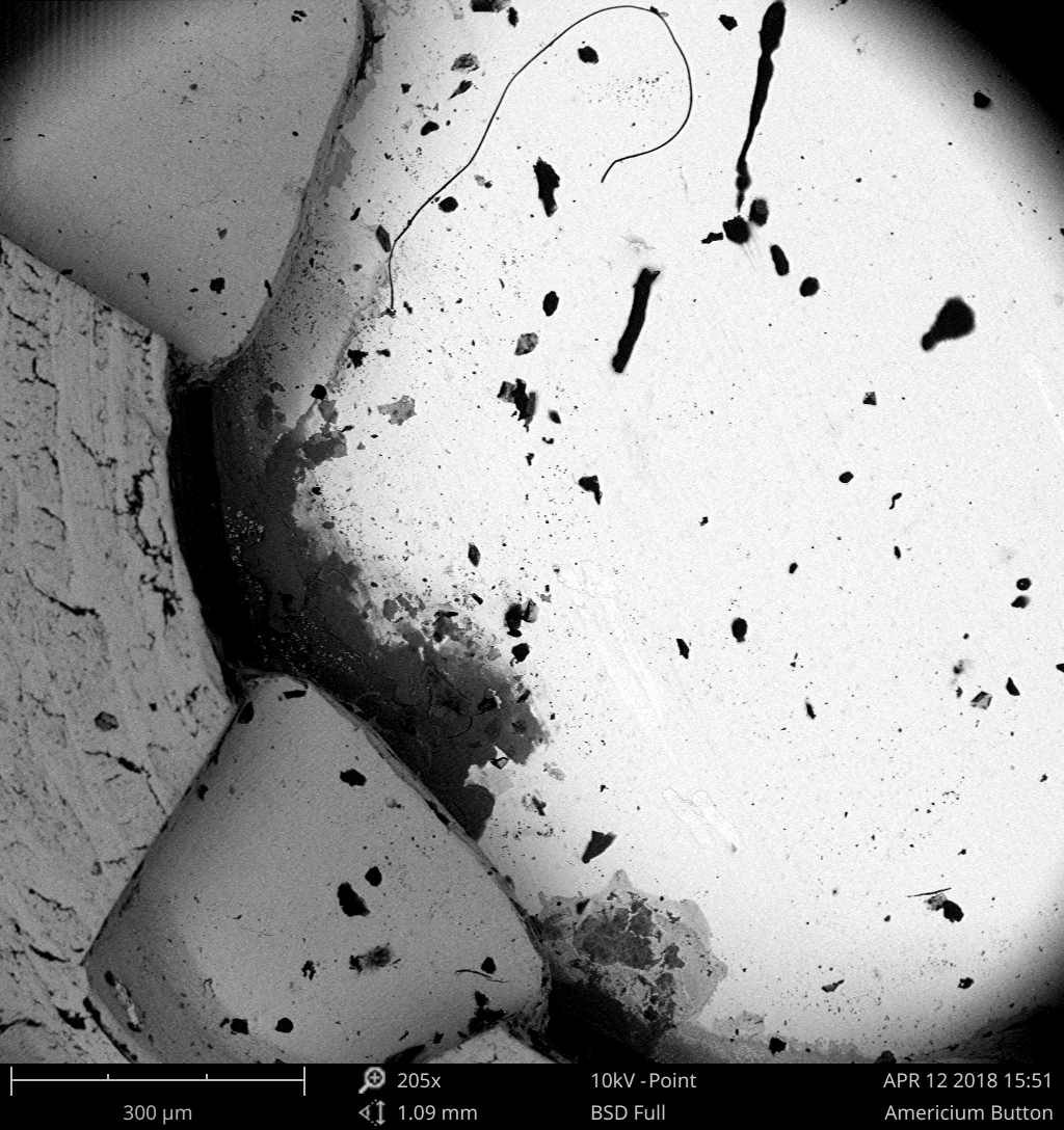
Starting in 2018 I spent a lot of time in front of three microscopes most people never get to touch. One was a scanning electron microscope (SEM), which sweeps a focused beam of electrons across a sample and builds a picture from the ones that scatter back. Another is the atomic force microscope (AFM), which sweeps an atomically-sharp vibrating cantilever across a surface and makes a picture from how the surface affects the vibrations. The last was a scanning tunneling microscope (STM), which drags a needle sharpened to a single atom so close to a surface that electrons leak across the gap. The SEM took me down to the micron. The AFM reveals surface details even finer. The STM took me the rest of the way, to single atoms.

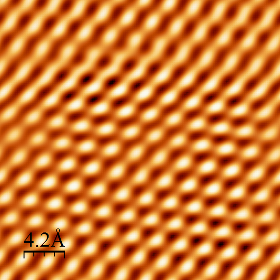
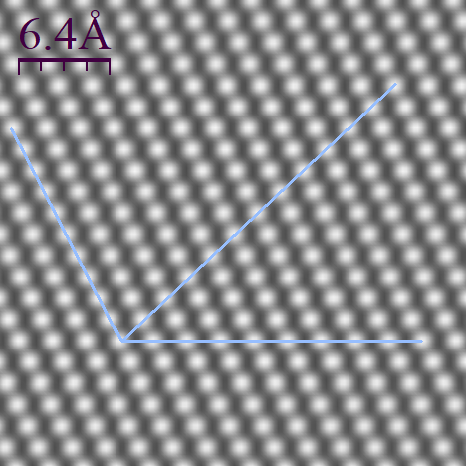
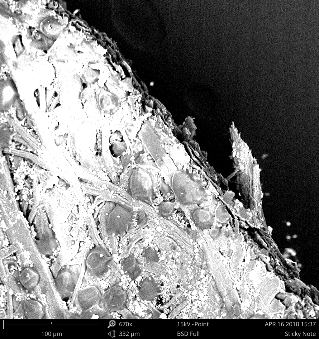
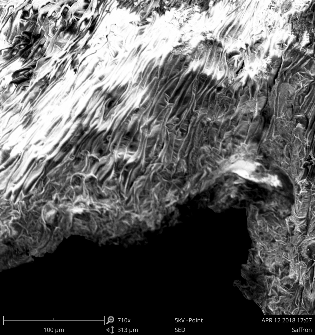
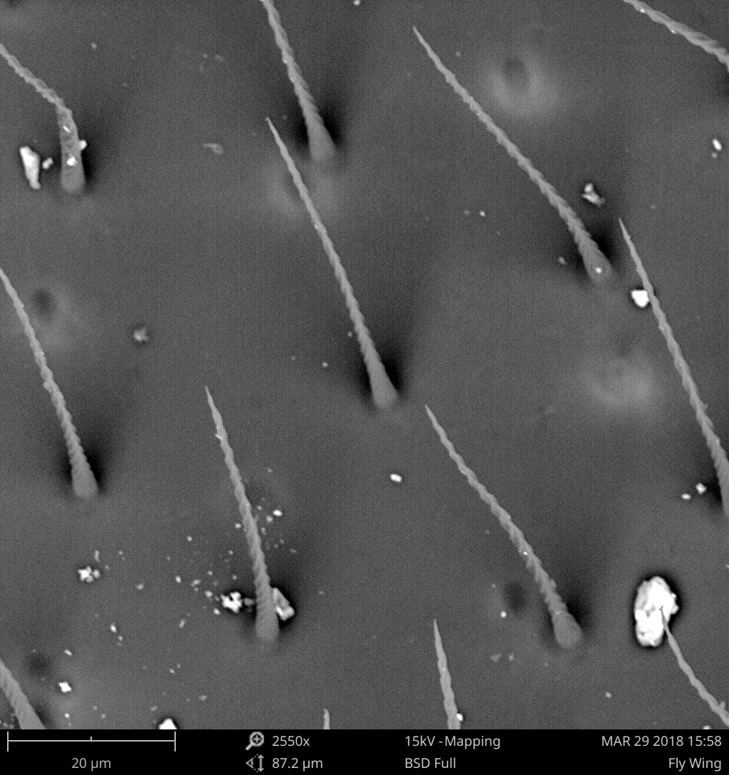
These are a selection of the images I took. The SEM images are grayscale because electrons carry no colorWhen we talk about color, we generally are talking about the perceptual response we have to our retina receiving photons of different energies. In this sense, electrons have no color, as our retinas aren’t sensitive to them; however, this shouldn’t be confused with saying the electrons are monochromatic — in physics, this word refers to the particles having a very tight, line-like energy spectrum (thereby consisting of effectively one energy, i.e. “color”), a property which is certainly not possessed by the backscattered electrons here.; the only thing added is the instrument’s own readout along the bottom edge of each one, with the scale bar, magnification, accelerating voltage, and the date I took it. The atomic scans at the end are false-colored by tunneling current (which is related to the height above the surface). Nothing else here is retouched.

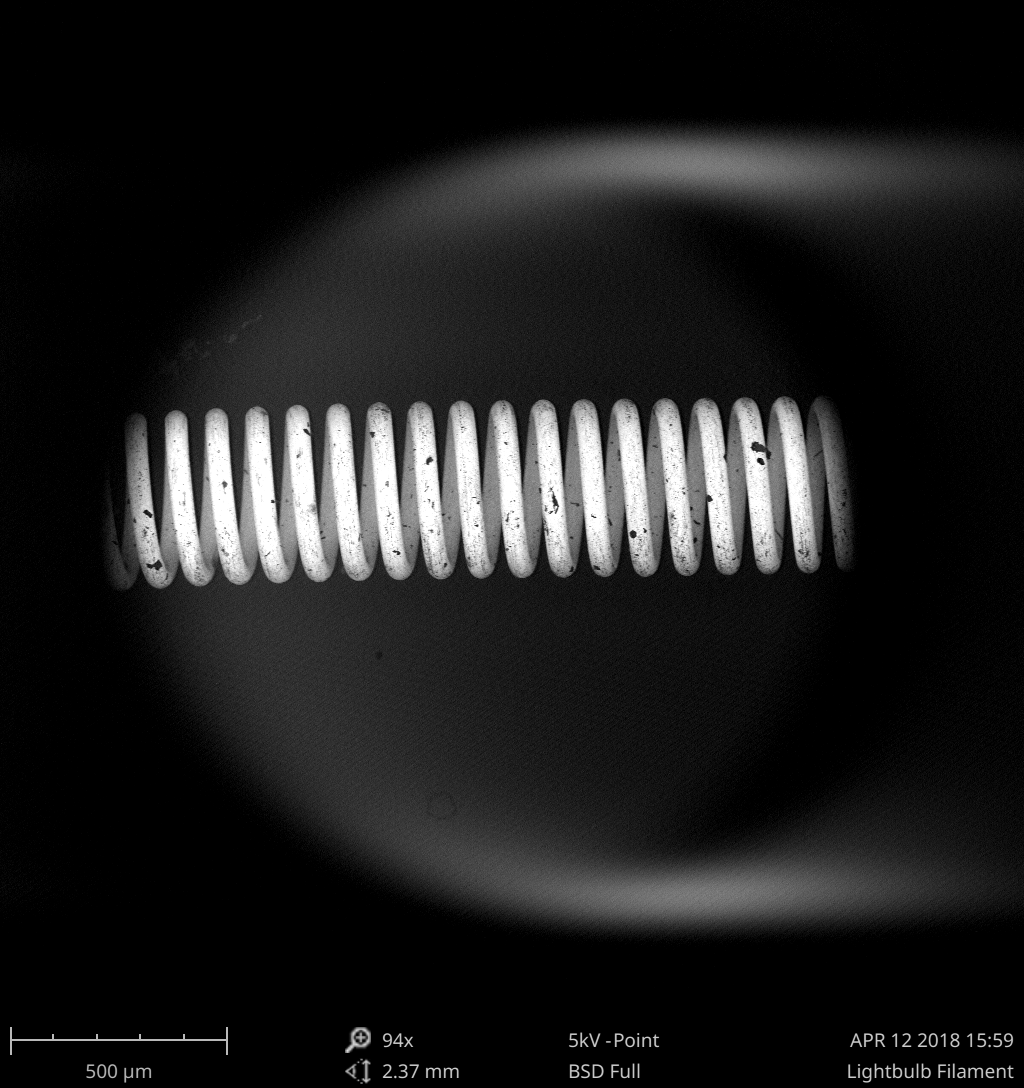
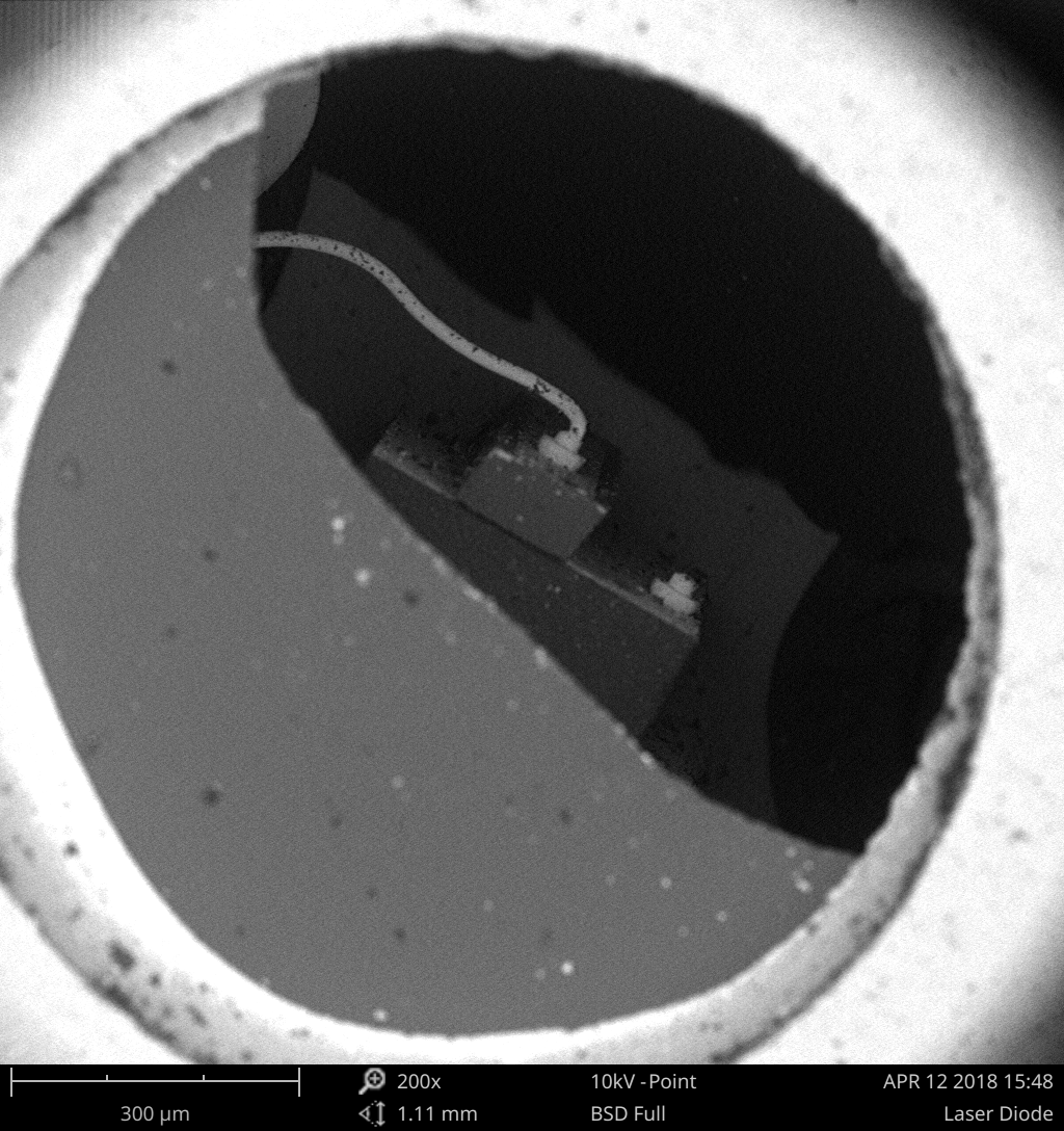
Under the electron beam
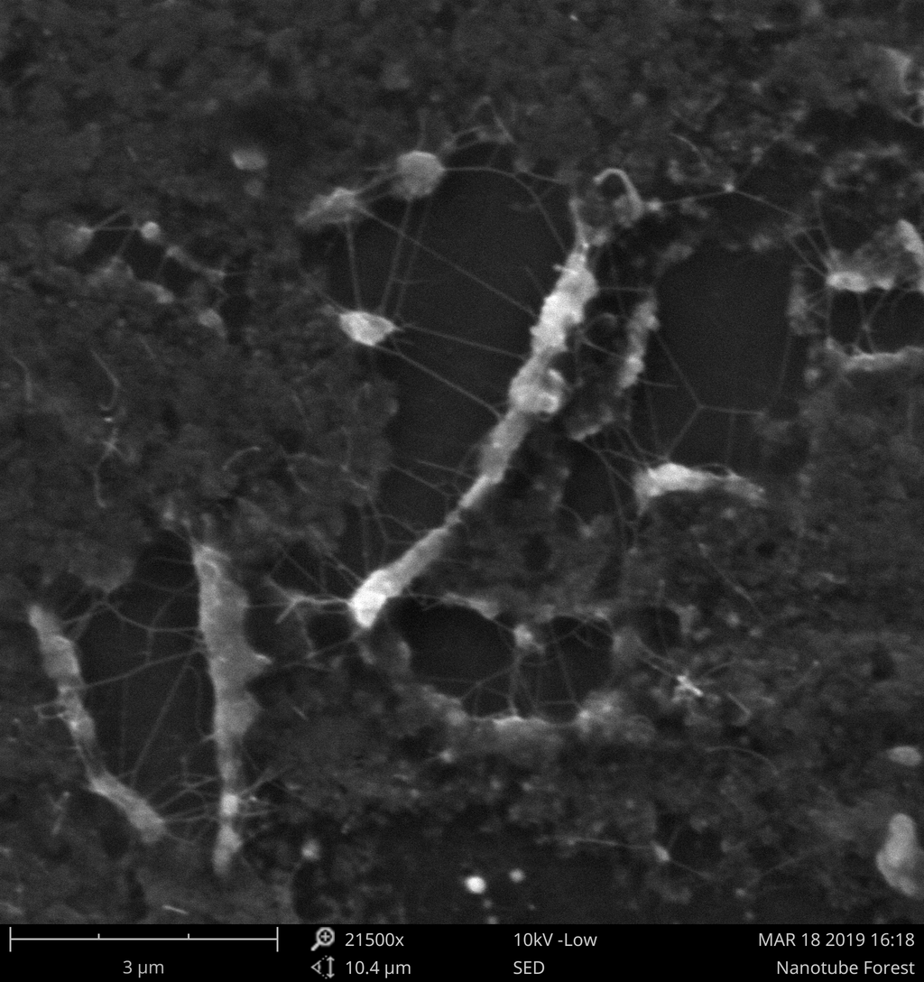
Scanning electron micrograph of a coiled tungsten lightbulb filament
A tungsten filament from an incandescent bulb: the coil that glows when you flip the switch, here cold and magnified about ninety times. At this low zoom, you can see the maximum scan window size of the electron beam — notice how it illuminates only a circular region, like a spotlight being shone.SEM · 94× · 5 kV · scale bar 500 µm
Close scanning electron micrograph of the tungsten filament wire showing it is a coiled coil
Closer in on a different style of filament, a commonly-used trick shows: it is a coiled coil, a fine helix of tungsten wound again into the larger spring, all to pack more glowing length into a small bulb. SEM · 890× · 15 kV · scale bar 80 µm
Scanning electron micrograph of a transmission electron microscope sample grid
A sample grid, the tiny mesh you mount a specimen on to look at it in a transmission electron microscope. Each window is a hundred microns across. SEM · 280× · 15 kV · scale bar 200 µm
Scanning electron micrograph of an atomic force microscope cantilever and tip
One microscope looking at another: this is the cantilever from an atomic force microscope, the diving board whose sharpened tip feels a surface atom by atom. SEM · 240× · 10 kV · scale bar 300 µm
Scanning electron micrograph of the cleaved end of an optical fiber
The cleaved end of a photonic-crystal fiber. SEM · 2300× · 10 kV · scale bar 30 µm
Scanning electron micrograph of a laser diode
A laser diode pulled from its housing. The light comes out of the small facet at the front, an aperture far smaller than the package built around it. SEM · 200× · 10 kV · scale bar 300 µm
Scanning electron micrograph of the adhesive microspheres on a Post-it note
The reason a Post-it sticks but peels off clean: its adhesive is a scatter of microscopic spheres, so only a fraction of the glue ever touches the paper. SEM · 670× · 15 kV · scale bar 100 µm
Scanning electron micrograph of a thread of saffron
A single thread of saffron, the dried stigma of a crocus flower and one of the most expensive things by weight you can buy. SEM · 710× · 5 kV · scale bar 100 µm
Scanning electron micrograph of a fly's wing
A fly's wing. What looks like a smooth membrane is ribbed and studded with fine hairs that comb the air. Notice the intricate structure each hair has.SEM · 2550× · 15 kV · scale bar 20 µm
Scanning electron micrograph of grains of table salt
Ordinary table salt. Sodium chloride cleaves along its cubic lattice, so even a kitchen grain breaks into sharp right-angled steps. SEM · 810× · 5 kV · scale bar 80 µm
Scanning electron micrograph of an americium-241 source button from a smoke detector
The americium-241 button from inside a household smoke detector. It steadily emits alpha particles, which ionize the air in the detector so a passing wisp of smoke can break the current. SEM · 205× · 10 kV · scale bar 300 µm
Scanning electron micrograph of carbon nanotubes
Carbon nanotubes, bright filaments threading across the substrate. The lab's standing line was that our instrument could not resolve these. As you can see, it turns out it could. SEM · SED · scale bar 3 µm
Felt, not seen

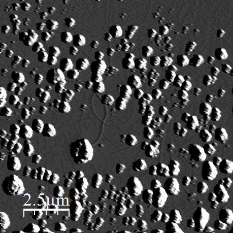
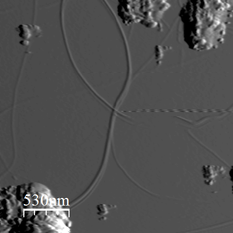
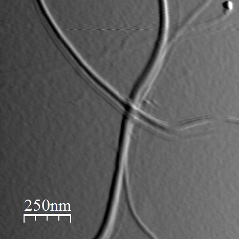
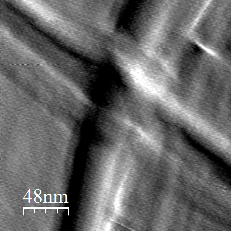
The atomic force microscope uses a different approach from the SEM. It uses no beam at all: a tip on the end of a tiny vibrating cantilever is dragged just above the surface, and the way the surface tugs on that vibration is read off as height, a true topographic map only nanometers tall. What follows is one continuous zoom, five frames walking in on a single patch of the same nanotube sample, from a few microns across down to a window only tens of nanometers wide.

Atomic force micrograph, widest view of the nanotube sample
The widest view: clumps of catalyst particles, the seeds the nanotubes grow from, scattered across the ultrapure silicon substrate. Even here you can see faint hints of CNTs. AFM · height · scale bar 4.6 µm
Atomic force micrograph zooming in on the nanotube sample
Closing in to about two and a half microns, the same scattered seeds with the threads between them starting to show more prominently. AFM · height · scale bar 2.5 µm
Atomic force micrograph of a nanotube on a flatter region
Down to half a micron. The clutter falls away and nanotubes come clearly into view, running across a comparatively flat stretch of surface. At this scale it becomes obvious that what previously looked to be single tubes are actually multiple lying side-by-side, traveling parallel to one another. AFM · height · scale bar 530 nm
Atomic force micrograph of multiple carbon nanotubes
Closer still: here the fine structure of the tubes becomes clearer. What appeared before to be only a few strands reveals itself to be a plethora. AFM · height · scale bar 250 nm
Atomic force micrograph, tightest view where nanotubes cross
The tightest frame, a window only tens of nanometers wide with the region where tubes cross filling most of it. This is about as far in as the tip can feel. AFM · height · scale bar 48 nm
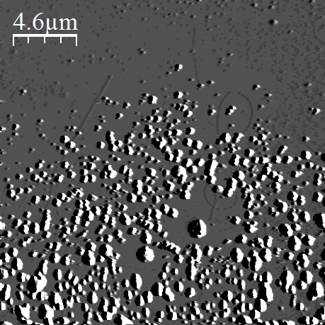
The atoms themselves

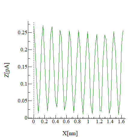
The electron microscope bottoms out around the micron. The AFM got us down to tens of nanometers. To go further, we can use quantum mechanics: bring a metal tip within a nanometer of a conducting sample, apply a small voltage, and a tunneling current flows across the vacuum gap. That current is so steep a function of distance that moving the tip by a single atom's width changes it measurably. RasterYou may wonder how it is even possible to build a motor which can position a tip with subnanometer precision. The answer is surprisingly simple: piezoelectrics. Using a crystal of material that changes its size in response to a voltage in a known way, you can reliably produce extremely fine-grained movements by applying precise voltages. the tip back and forth, and measure the tunneling current at each position to get an indicator of how far you are from the surface.

Scanning tunneling micrograph resolving individual carbon atoms on graphite, false-colored
The surface of graphite, atom by atom. Each bright bump is a single carbon atom; the rows repeat every couple of ångströms. The scale bar reads 4.2 Å, less than half a nanometer across the whole marker. STM · HOPG graphite · tunneling current false-colored
Grayscale scanning tunneling micrograph of the graphite atomic lattice
The same lattice in grayscale, scale bar 6.4 Å. Graphite famously hands the STM only every other atom, so the surface reads as a triangular pattern rather than a full honeycomb, with a spacing of about 0.24 nm. STM · HOPG graphite
Line profile across the graphite surface showing periodic atomic corrugation
Proof it is not noise: a single line dragged across the surface. The tunneling current rises and falls in a clean periodic wave, one bump per atomic row, the corrugation measured in tenths of a nanometer. STM · tunneling current vs. position along one scan line