Verification of the value of the conductance quantum 2e²/h
Originally written for PHYS 4410 (Advanced Experimental Physics) at Cornell University. Download the original paper (PDF).
Abstract. The quantum of conductance is measured experimentally using the method of Au–Au breakjunctions, and is verified to have value within 15% of theoretical \(2e^2/h\).2026 note. The 15% quoted here is the spread of the per-quantum measurements (a sample standard deviation of \(0.15\,G_0\)), not the disagreement of the result with theory. The mean agrees far more tightly, to about 0.4% (\(0.9959\,G_0\), reported in the discussion and conclusion). The existence of an effective series resistance due to backscattering of charge carriers off the junction is confirmed, and deviations from values found in the literature are discussed. It is noticed that correction for backscatter is not required when selecting for pristine samples, and possible mechanisms for this are proposed.
Introduction
It is well-known that conductance at a quantum point contact becomes quantized.1 This quantization is one of the few examples of quantum effects which are apparent at the macroscopic scale at room temperature. The phenomenon has been reported in countless experiments, and the value of the quantum measured using a variety of methods.
As the world grows increasingly dependent on small-scale technologies such as computer processors, and interest in nanotechnology increases, it will become important to understand completely the electrical properties of wires at this scale. Connecting traces in silicon are rapidly approaching the scale of atoms, and there are situations where the assumption of conductivity varying continuously with geometry may not be valid.
This experiment aims to demonstrate a situation in which this assumption is indeed broken, and conductivity becomes quantized. In addition, the value of the quantum will be determined and compared to expected values from the literature.
Experimental setup and methods
There are many methods through which the quantization of conductance can be measured. In this experiment, the method employed is that of the gold breakjunction. Two gold wires are slowly brought into or out of contact with one another. As they form or break a junction, they form a quantum point contact. During these moments, I wish to measure the conductivity of the junction.
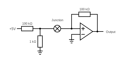
To enable this, a fixed potential will be placed across the junction. I start with a supply potential of \(5\,\mathrm{V}\). This is too high to place across the junction directly, as it may cause heating issues or cause loss of signal into noise. Instead, a divider network of \(100\,\mathrm{k}\Omega\) and \(1\,\mathrm{k}\Omega\) are employed to reduce the supply potential to a nominal \(50\,\mathrm{mV}\).
The wire junction is mounted with one wire fixed, and the other able to be raised or lowered with a screw. This allows fine tuning the distance between them. One wire is connected to the \(50\,\mathrm{mV}\) potential, and the other to the non-inverting input of an operational amplifier configured as a transimpedance amplifier. A feedback resistor with a value of \(100\,\mathrm{k}\Omega\) is chosen. The amplifier output is monitored using a USB digital storage oscilloscope. A diagram of the circuit is available in the figure below.
The wires are brought into contact, and very slowly separated. The moment they do, the table is tapped to see if ambient vibrations can cause the wires to contact again. The process is repeated until tapping the table is able to break and restore connection between the wires reliably.
The oscilloscope is set to trigger on falling edges, so that it will start sampling when a contact is formed. Many thousands of such traces are recorded for analysis.
Analysis
The conductance quantum is expected to have a value of \(G_0=2e^2/h\approx77.48\,\mu\mathrm{S}\). The \(50\,\mathrm{mV}\) potential difference in use will induce a current of \(G_0(50\,\mathrm{mV})\) across a single quantum. This is roughly \(3.87\,\mu\mathrm{A}\). The transimpedance amplifier has a transimpedance of \(100\,\mathrm{mV}\,\mu\mathrm{A}^{-1}\), meaning I expect plateaus at roughly \(387\,\mathrm{mV}\) on the oscilloscope.
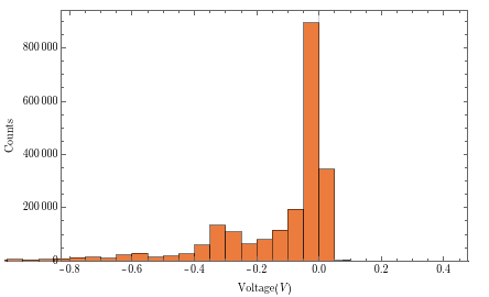
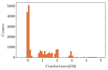
All data analysis was performed in Mathematica. Traces were imported into the software, and some basic data scrubbing is done. As a first visual inspection, each measured voltage sample is plotted on a histogram, from all traces. The disconnected state is most prominent, but there is an obvious secondary peak, and potential evidence of a third.
To attempt to remove bad traces, I plot histograms for each captured trace individually, and note which have visually obvious multiple peaks. These traces are then pulled from the batch, and merged together. The voltages are converted into units of \(G_0\) through the same relationship described above. A histogram of this data can be seen below.
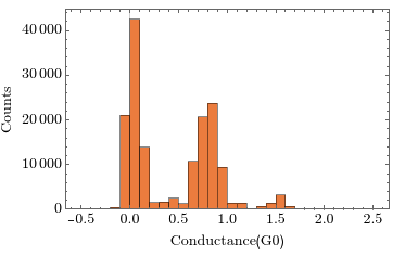
Notice, the peaks do not appear to line up with integer multiples of the conductance quantum. Reports in the literature also find this effect, and suggest backscattering of the electrons at the junction is responsible.2 The backscattering can be modeled as an additional series resistance \(R\):
$$\begin{aligned} \frac{1}{G_{obs}}&=\frac{1}{G_{junc}}+R\\ \implies \frac{G_{junc}}{G_0}&=\frac{1}{\frac{G_0}{G_{obs}}-RG_0} \end{aligned}$$
The literature reports typical values of \(R\) to be of order \(400\,\Omega\).3 To determine a best fit model resistance, a scoring function \(f(R)\) is described:
$$f(R)=\sum_i\left|G_i(R)-\lfloor G_i(R)\rceil\right|$$
Where \(i\) is a sample index, \(G_i(R)\) is the computed junction conductance for a model series resistance \(R\), and \(\lfloor\lambda\rceil\) is the function which rounds to nearest integer. This scoring function measures the total distance of all samples from the nearest integer, and Mathematica is used to minimize with respect to \(R\).
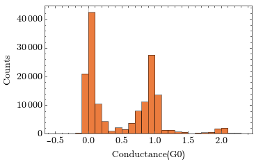
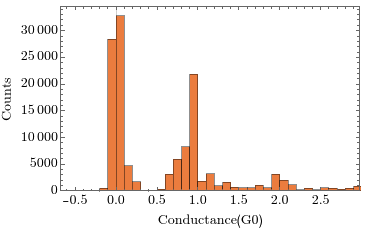
Doing so results in \(R\approx2.3\,\mathrm{k}\Omega\). The corrected histogram can be seen below.
As a test of this series resistance being some function of the physical set up, another batch of traces is selected from the dataset. The two batches have no traces in common. These are then corrected for using the same series resistance found for the previous batch, and a histogram is made.
One final batch of traces is made, consisting of only traces of exceptional quality. This is determined essentially subjectively, by eye. Defining traits which make a trace “exceptional” include sharp transitions, flat plateaus, and long plateaus. An example of such a trace can be seen below.
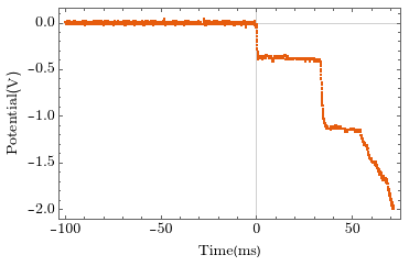
Fewer traces of this quality are available, and the sample counts in the histogram will reflect this. A histogram is made from these traces, as before. However, this time no series resistance correction will be applied.
Note that despite no correction, the peaks neatly align with integer multiples of the conductance quantum.
Discussion
With the first batch of traces, I find a large shift between the observed and expected values of the conductance quantum. Review of the literature suggests this is a documented and common effect, caused by electrons backscattering from the junction. As shown in the analysis, this backscattering can be modeled by the addition of a series resistance to the full circuit. In doing, I find the value of the resistance to be substantially larger than previous findings suggest, at \(\sim2.3\,\mathrm{k}\Omega\).
I offer a potential explanation for this discrepancy. The quantization of conductance across a junction is caused by ballistic transport of the charge carriers. Ballistic transport requires transmission probability going to unity. However, if the charge carriers have high momenta, their scattering cross-section at the junction can increase substantially due to the carrier wavelengths approaching from above the size of characteristic lengths of the junction. In the future, the analysis could be repeated for varying potentials across the junction. If the above mechanism is responsible, I expect to see \(R\propto V_{in}\) to first order.
After eliminating data that lies \(<\frac{1}{2}G_0\), and then cutting into bins centered at \(nG_0\) for integer \(n\) which extend from \(nG_0-\frac{1}{2}G_0\) to \(nG_0+\frac{1}{2}G_0\), the bins are stacked. The mean is then found to be \(0.9959G_0\), with standard deviation \(0.15G_0\). This shows reasonable agreement with the expected value.
An interesting observation can be made of the highly-curated traces, whose data is visible in the final histogram above. Despite having had no corrections made to the recorded data, alignment with the integral multiples of the conductance quantum is easily visible. This would seem to not be in agreement with the proposed increased backscatter amplitude mechanism I proposed above. I wonder if it is possible that this effect has been removed by my selection process. The scattering is a probabilistic process, and perhaps backscatter is responsible for making the transitions between plateaus on a trace blurred. If this is true, then transitions where no backscatter occurs would be very sharp and defined – precisely the condition I selected for in this batch’s traces. I think tighter experimental controls would be required to test these ideas more thoroughly.
Conclusion
The value of the quantum of conductance was measured through the method of Au–Au breakjunctions, and found to be \(\left(0.9959\pm0.15\right)\frac{2e^2}{h}\).
The existence of an additional effective series resistance, presumably due to backscattering of electrons, is confirmed as well. Its value is measured to be approximately \(2.3\,\mathrm{k}\Omega\), which differs substantially from the literature which reports values of order \(400\,\Omega\). Increase in scattering amplitude due to decrease in wavelength of the charge carriers was proposed as a potential mechanism.
Finally, it was noticed that this series resistance correction does not appear to be necessary when only traces of pristine quality are selected for. A potential reason for this was suggested to be that backscatter of charge carriers is responsible for the blurred transitions between quanta.
-
Y. Kurui, Y. Oshima, M. Okamoto, and K. Takayanagi. Conductance quantization and dequantization in gold nanowires due to multiple reflection at the interface. Phys. Rev. B, 79(16):165414, 2009. ↩
-
P. García-Mochales, P. A. Serena, N. García, and J. L. Costa-Krämer. Conductance in disordered nanowires: forward and backscattering. Phys. Rev. B, 53(15):10268–10280, 1996. ↩
-
E. L. Foley, D. Candela, K. M. Martini, and M. T. Tuominen. An undergraduate laboratory experiment on quantized conductance in nanocontacts. Am. J. Phys., 67(5):389–393, 1999. ↩
Errata
- 2026-06-05 — Corrected four grammatical slips present in the original (“measured experimental” → “experimentally”; “able to raised or lowered” → “able to be raised or lowered”; “showing the all circuit elements” → “showing all the circuit elements”; and a “than” → “then” in the discussion). The prose is otherwise reproduced as written.